| Type | Positive | Negative |
| TL071 | FET-input type, very low bias, cheap | several mV offset wich must be trimmed, "high" noise |
| TL072/74 | FET-input type, very low bias, cheap | several mV offset wich cannot be trimmed directly, "high" noise |
| OPA134 | FET-input type, very low bias | several mV offset wich must be trimmed directly, "high" noise, expensive |
| OPA134 | FET-input type, very low bias | several mV offset wich cannot be trimmed directly, "high" noise, expensive |
| OPA604 | FET-input type, very low bias | several mV offset wich must be trimmed directly, "high" noise, expensive |
| OPA2604 | FET-input type, very low bias | several mV offset wich cannot be trimmed directly, "high" noise, expensive |
| OPA197/2197 | Very low bias, Low noise, low offset | expensive |
| TLV07 | Very low bias, Low noise, low offset | Attention on Vcc and differential input voltage ! |
| L293 | ST | DIL, good and available | 2,00 € |
| L298 | ST | SMD + TO220-11 | 2,40 € / 6,30 € |
| L6202 | ST | DIL | 3,85 € |
| ZXMHC6A07T8TA | Zetex | SMD H Bridge FETs | 1,15 € |
| DRVxxx | TI | cheap at Mouser, not available at smaller stores | |
| LB 1641 | Sanyo | cheap, SIL (THT), no further info | 1,25 € |
| A3967 | Allegro | SMD | 2,99 € |
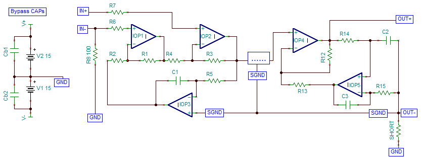
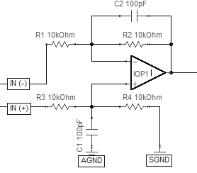
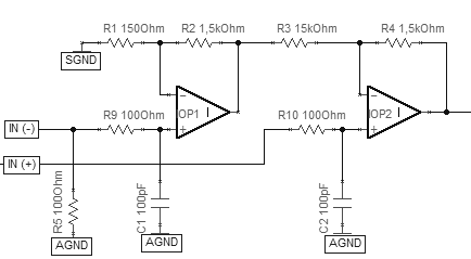
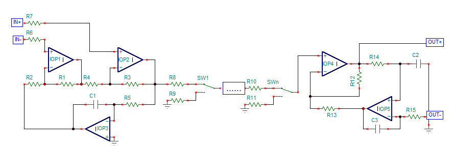
 This
(classic) approach gives
high input impedance and good CMMR, if the resistors R1...R4 are 0.1%
tolerance.
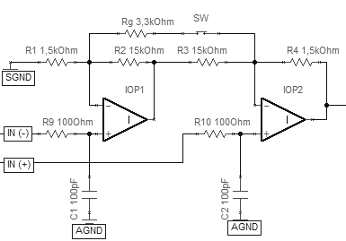
This
(classic) approach gives
high input impedance and good CMMR, if the resistors R1...R4 are 0.1%
tolerance.| Circuit | Output noise [µVrms] |
Output noise [dBu] |
Output noise [dB] rel. 1Vrms @ input |
Pro/CON |
| One OPamp simple input stage, gain = 1.0 | 4,2 | - 105,3 | - 107,5 | - high noise + 1 OPamp + gain < 1 possible |
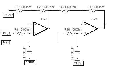
| Three OPamp Input Stage, gain = 1.0 | 2,4 | - 110,2 | - 112,4 | - high noise - 3 OPamps + gain < 1 possible |
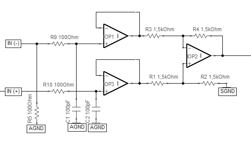
| Two OPamp input stage (standard), gain = 2.0 | 2,7 | - 109,2 | - 117,4 | - high output voltage + good noise |
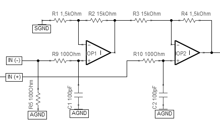
| * Two OPamp input stage (low gain), gain = 1.1 | 1,6 | - 113,7 | - 116,8 | + good noise |
| * Two OPamp input stage (low gain, switchable), gain = 2.0 | 2,7 | - 109,2 | - 117,4 | + good noise |
| Two OPamp input stage (low gain, low noise), gain = 1.1 | 1,5 | - 114,3 | - 117,3 | - low
resistor values + best noise |
| Two OPamp input stage (low gain, low noise), gain = 2.0 | 2,5 | - 109,8 | - 118,1 | - high output voltage - low resistor values + best noise |
| Gain | Output noise [µVrms] |
Output noise [dBu] |
Output noise [dB] rel. 1Vrms @ OutStage input |
Output
noise
[dB] rel. 100mVrms @ OutStage input |
| gain = 1.2 (+1,6 dB) | 1,32 | - 115 | - 119,3 | - 99,3 |
| gain = 2.0 (+6,0 dB) | 1,94 | - 112 | - 120,2 | - 100,2 |
| gain = 2.4 (+7,6 dB) | 3,04 | - 108 | - 117,9 | - 97,9 |